Slingshot
A battery-powered sensor pod worn on an upper-arm compression sleeve that turns a training session into data, fusing motion and heart-rate into a single Session Load Score, plus jump count, vertical, and heart-rate intensity zones. As co-founder and Co-CTO, one of just two engineers on the team, I own the hardware and embedded systems end to end: schematic capture, PCB layout, fabrication, assembly, and firmware bring-up of a matchbook-sized mixed-signal board.
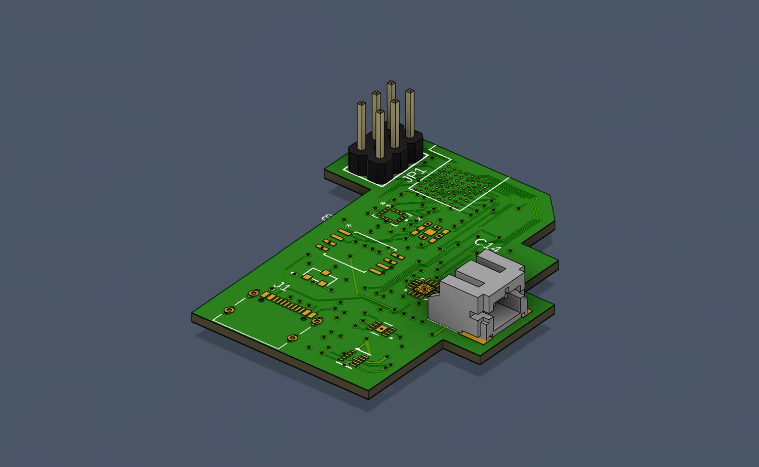 Drag to rotate
Most of the engineering difficulty here is coexistence: a 2.4 GHz radio, a switching power supply, and a microvolt-level optical heart-rate front end all have to share one matchbook-sized board without corrupting each other. The design is built around protecting RF range and signal quality while still fitting a full sensor suite, on-board logging, and a complete battery-management chain.
Smaller, denser, in manufacturing now
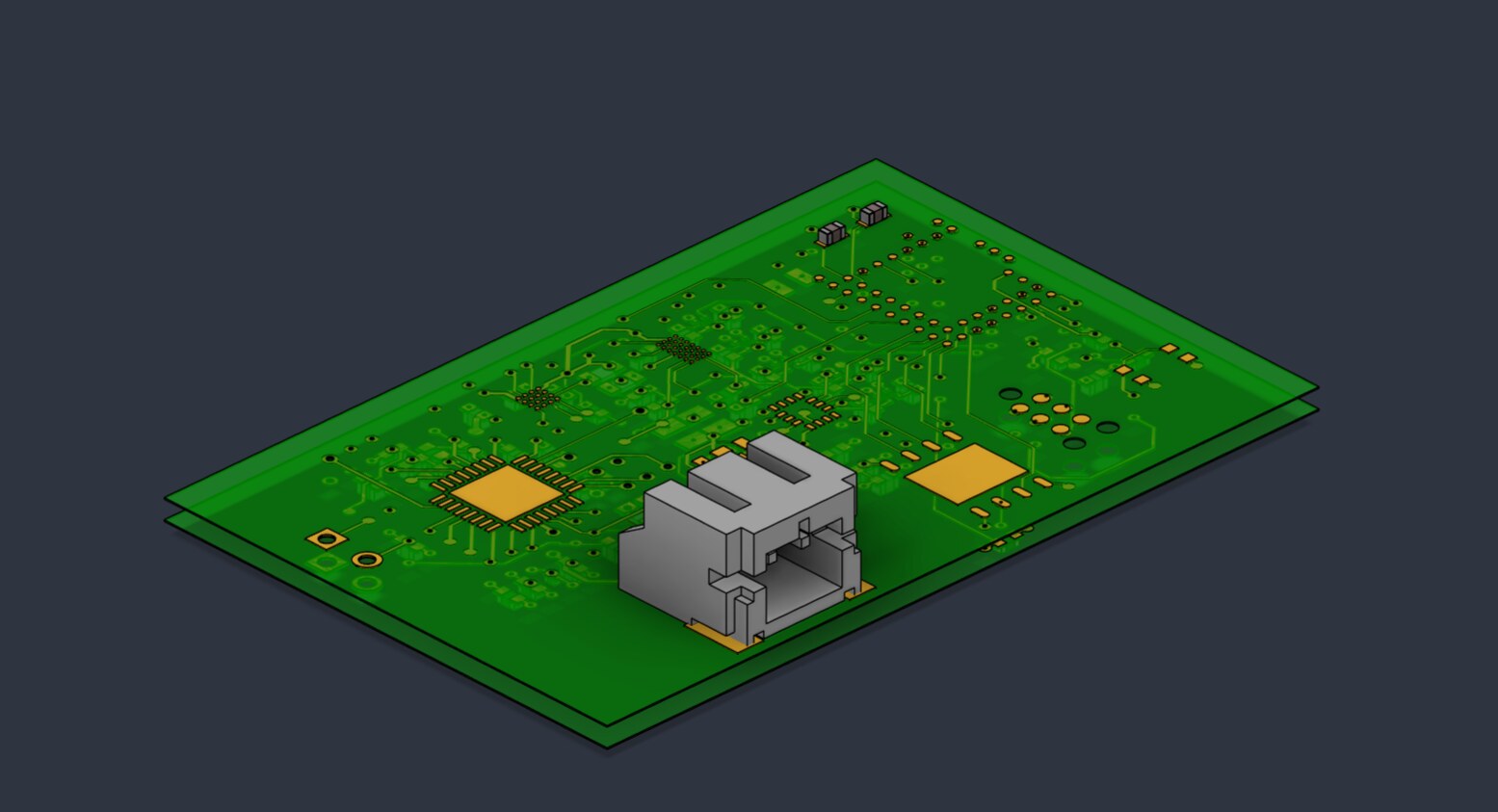
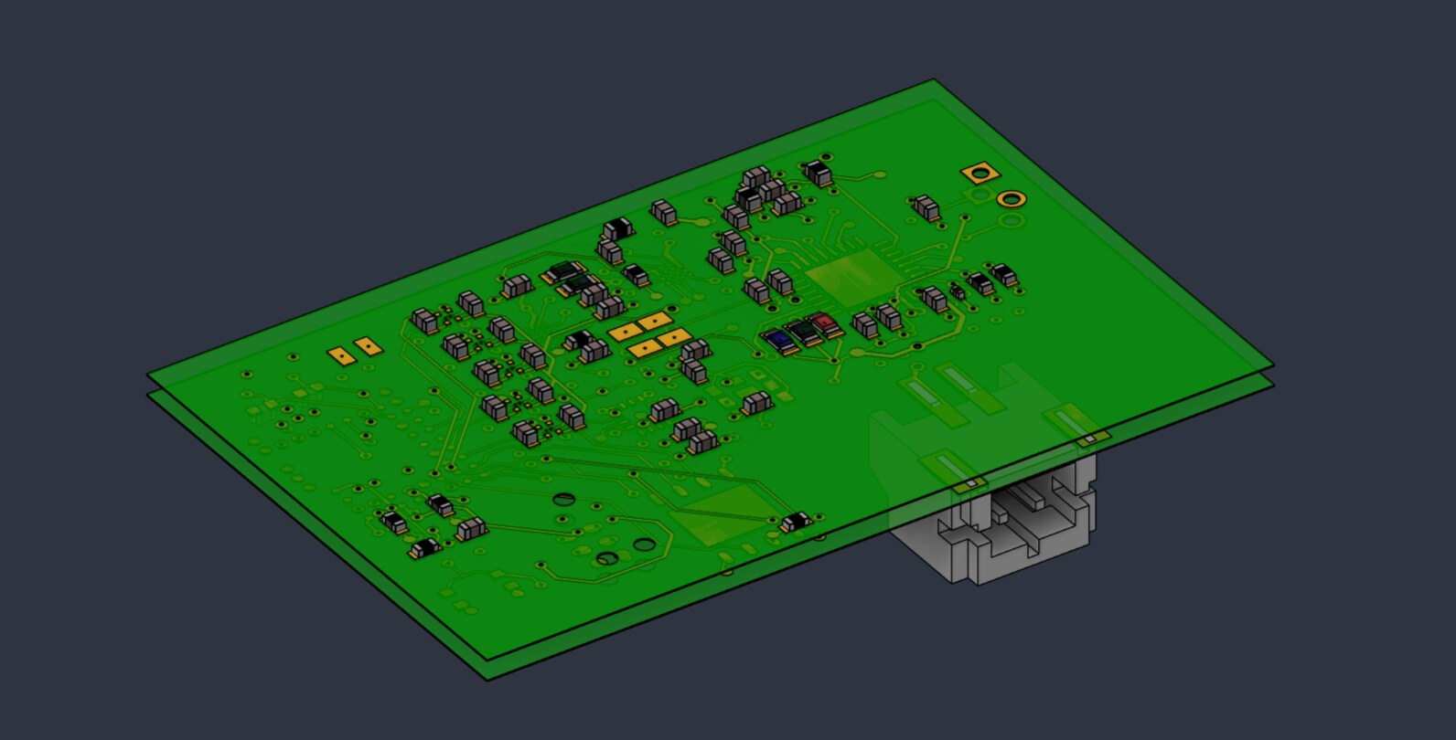
3D renders of the V2 design currently being built at a new factory. V2 folds V1's four discrete power ICs into one nPM1300 PMIC, swaps the nRF52840 module for the smaller nRF54L15 module, and moves the whole board to ball-grid packages that get placed by machine and X-ray-inspected. (Renders only, schematics, layout, and Gerbers stay in-house.) Tap either to enlarge.
What V1 taught us, and what V2 changed
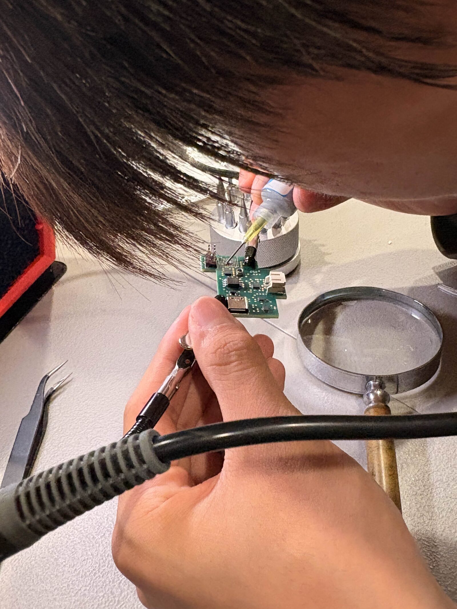
All five V1 boards came back from the fab clean and failed to come up on the bench after we hand-reflowed the radio module onto them ourselves, traced back to that hand-soldering step rather than a layout or fab defect. That's a real cost of hand-assembling a fine-pitch board on our own bench. It's a direct reason V2 assembly moved to a contract manufacturer with reflow ovens and X-ray inspection instead of staying on our bench. In parallel, V2 was drawn against the honest list of what designing V1 already taught us to change, and is now in production at that new factory (the first one couldn't hit our summer schedule).
Power — four chips to one
- V1 spread power across four chips: charger, buck-boost, 1.8 V regulator, fuel gauge.
- V2 folds all four into a single nPM1300 PMIC made for wearables — less board area, fewer ways to be wrong.
Radio — nRF52840 → nRF54L15
- Kept it as a pre-certified module rather than a bare chip; own RF certification would cost more time than the size saved.
- Smaller footprint, newer core, same BLE toolchain path.
Charging & data — magnetic + BLE
- V1 charged and moved data over USB-C. V2 drops the port.
- Charging → sealed two-pin magnetic connector; data → off the board over BLE, the path the live app needs anyway. Survives sweat and a gym floor.
Assembly — smaller packages, X-ray
- V2 uses parts whose connections sit under the chip instead of along the edges (BGA/WLCSP).
- Placed by machine, checked by X-ray, unreworkable by hand. We kept the flash memory in an older larger package on purpose, so at least one chip can still be lifted at the bench.
The full public build log lives at slingshot-sports.com/buildlog.
The power tree, collapsed into one chip
V1 spread charging, buck-boost regulation, a small 1.8 V rail, and fuel gauging across four discrete ICs. V2 folds all four functions into a single Nordic nPM1300 PMIC designed for wearables at this size — same power tree, fewer parts, less area, fewer ways to be wrong.
Why buck-boost, not an LDO: a single Li-Po swings roughly 3.0–4.2 V, which crosses the 3.3 V output. A buck-boost holds the rail steady across the whole discharge curve where a buck or LDO would sag — a topology choice driven by the battery's behavior, with the switch-node loop kept tight and well away from the radio and the optical front end.
Five-sensor suite
Fused over I²C / SPI / QSPI and read by the nRF52840, which logs to flash and streams telemetry over BLE.
What I own, end to end
Hardware / PCB
- Designed a 4-layer mixed-signal stackup (Top / GND / 3V3 / Bottom) in Fusion Electronics; fabricated & assembled at JLCPCB.
- Managed RF + switching-supply + sensitive-analog coexistence on one matchbook-sized board.
- Owned BOM, sourcing, and DFM, basic vs. extended parts, CPL rotations, JLCPCB rules, and checked board-to-enclosure fit via ECAD↔MCAD.
Power electronics
- Architected the full power tree: BQ24074 → TPS63802 → 3.3 V (+1.8 V), MAX17048 on the battery node.
- Chose buck-boost over an LDO to hold 3.3 V across the whole Li-Po discharge curve.
- Applied switching-layout discipline to protect both RF range and heart-rate signal quality.
Firmware
- Embedded C/C++ on PlatformIO + nRF52 Arduino core for the nRF52840, two build environments (dev kit + custom board).
- One codebase, two data paths: flash logging + USB-CDC dump (v1) and BLE streaming (v2), additive, no rewrite.
- Built a synthetic "demo stream" to validate capture → packetize → stream before sensors were wired; SWD/J-Link via nRF52840-DK.
Design review & V2 respin
- Caught an nRF52840 VDDH/VDD power-mode conflict and a switching-regulator feedback-divider error before fab, both the kind of mistake that kills a board and costs a multi-week respin.
- Drove the V2 respin at a new manufacturer: ~500 DRC violations resolved on 0.35 mm-pitch WLCSP/BGA via via-in-pad escape routing; five units in factory build with flying-probe test.
- Routed every datasheet number — pins, registers, electrical limits — to verification rather than memory. Built in observability: rail test points and a debug header so a non-booting board isn't a black box.
Beyond the board
The pod is only half the product. I also built the software that turns its data into something a coach can use.